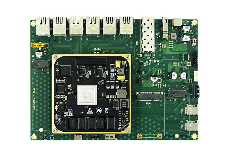
Artificial intelligence 8 layer pcb with vais in pad tech
Loading...
Artificial intelligence 8 layer pcb with vais in pad tech
Product Name: AI 8 Layer PCB with VAIS in pad tech
Description: We are a factory specializing in producing advanced AI 8 layer PCB with VAIS in pad technology. Contact us for high-quality electronic components.
Product Material As a supplier of various PCB technologies, volumes, lead time options, we have a selection of standard materials with which a large bandwidth of the variety of types of PCB can be covered and which are always available in house. Requirements for other or for special materials can also be met in most cases, but, depending upon the exact requirements, up to about 10 working days may be needed to procure the material. Do get in touch with us and discuss your needs with one of our sales or CAM team. Standard materials held in stock:
Components
Thickness
Tolerance
Weave type
Internal layers
0,05mm
+/-10%
106
Internal layers
0.10mm
+/-10%
2116
Internal layers
0,13mm
+/-10%
1504
Internal layers
0,15mm
+/-10%
1501
Internal layers
0.20mm
+/-10%
7628
Internal layers
0,25mm
+/-10%
2 x 1504
Internal layers
0.30mm
+/-10%
2 x 1501
Internal layers
0.36mm
+/-10%
2 x 7628
Internal layers
0,41mm
+/-10%
2 x 7628
Internal layers
0,51mm
+/-10%
3 x 7628/2116
Internal layers
0,61mm
+/-10%
3 x 7628
Internal layers
0.71mm
+/-10%
4 x 7628
Internal layers
0,80mm
+/-10%
4 x 7628/1080
Internal layers
1,0mm
+/-10%
5 x7628/2116
Internal layers
1,2mm
+/-10%
6 x7628/2116
Internal layers
1,55mm
+/-10%
8 x7628
Prepregs
0.058mm*
Depends on layout
106
Prepregs
0.084mm*
Depends on layout
1080
Prepregs
0.112mm*
Depends on layout
2116
Prepregs
0.205mm*
Depends on layout
7628
Cu thickness for internal layers: Standard - 18µm and 35 µm, on request 70 µm, 105µm and 140µm Material type: FR4 Tg: approx. 150°C, 170°C, 180°C εr at 1 MHz: ≤5,4 (typical: 4,7) More available on request Stackup A standard 8 layer PCB stackup is an 8 PCB board. It consists of the outer and inner signal layers and has many layersinside of it to prevent signal crosstalk. The layers of 8 layer PCB stackup are as follow: ·Toplayer ·Silkscreenlayer ·Solder masklayer ·High-speed signallayer ·Signal layer ·Powerlane ·Ground layer There are 7 layers of dielectric that connectfour ground planes to four signal layers.