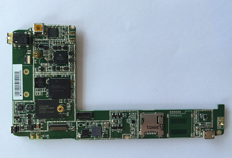
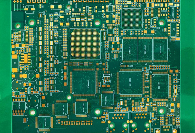
IntroductionHDI is an abbreviation for High-Density Interconnect. It is a complex PCB design technique. HDI PCB technology can shrink printed circuit boards in the PCB field. The technology also provides high performance and greater density of wires and circuits.By the way, HDI circuit boards are designed differently than normal printed circuit boards.HDI PCBs are powered by smaller vias, lines and spaces. HDI PCBs are very lightweight, which is closely related to their miniaturization.On the other hand, HDI is characterized by high frequency transmission, controlled redundant radiation, and controlled impedance on the PCB. Due to the miniaturization of the board, the board density is high.Microvias, blind and buried vias, high performance, thin materials and fine lines are all hallmarks of HDI printed circuit boards.Engineers must have a thorough understanding of the design and HDI PCB manufacturing process. Microchips on HDI printed circuit boards require special attention throughout the assembly process, as well as excellent soldering skills.In compact designs like laptops, mobile phones, HDI PCBs are smaller in size and weight. Due to their smaller size, HDI PCBs are also less prone to cracks.HDI Vias Vias are holes in a PCB that are used to electrically connect different layers in the PCB. Using multiple layers and connecting them with vias reduces PCB size. Since the main goal of an HDI board is to reduce its size, vias are one of its most important factors. There are different types of through holes.Through hole viaIt goes through the entire PCB, from the surface layer to the bottom layer, and is called a via. At this point, they connect all layers of the printed circuit board. However, vias take up more space and reduce component space.Blind viaBlind vias simply connect the outer layer to the inner layer of the PCB. No need to drill the entire PCB.Buried viaBuried vias are used to connect the inner layers of the PCB. Buried vias are not visible from the outside of the PCB.Micro viaMicro vias are the smallest via size less than 6 mils. You need to use laser drilling to form micro vias. So basically, microvias are used for HDI boards. This is because of its size. Since you need component density and cannot waste space in an HDI PCB, it is wise to replace other common vias with microvias. Additionally, microvias do not suffer from thermal expansion issues (CTE) because of their shorter barrels.StackupHDI PCB stack-up is a layer-by-layer organization. The number of layers or stacks can be determined as required. However, this could be 8 layers to 40 layers or more. But the exact number of layers depends on the density of the traces. Multilayer stacking can help you reduce PCB size. It also reduces manufacturing costs. By the way, to determine the number of layers on an HDI PCB, you need to determine the trace size and the nets on each layer. After identifying them, you can calculate the layer stackup required for your HDI board.Tips to design HDI PCB• Precise component selection. HDI boards require high pin count SMDs and BGAs smaller than 0.65mm. You need to choose them wisely as they affect via type, trace width and HDI PCB stack-up.• You need to use microvias on the HDI board. This will allow you to get double the space of a via or other.• Materials that are both effective and efficient must be used. It is critical to the manufacturability of the product. • To get a flat PCB surface, you should fill the via holes.• Try to choose materials with the same CTE rate for all layers.• Pay close attention to thermal management. Make sure you properly design and organize the layers that can properly dissipate excess heat.


 Through hole via It goes through the entire PCB, from the surface layer to the bottom layer, and is called a via. At this point, they connect all layers of the printed circuit board. However, vias take up more space and reduce component space. Blind via Blind vias simply connect the outer layer to the inner layer of the PCB. No need to drill the entire PCB. Buried via Buried vias are used to connect the inner layers of the PCB. Buried vias are not visible from the outside of the PCB. Micro via Micro vias are the smallest via size less than 6 mils. You need to use laser drilling to form micro vias. So basically, microvias are used for HDI boards. This is because of its size. Since you need component density and cannot waste space in an HDI PCB, it is wise to replace other common vias with microvias. Additionally, microvias do not suffer from thermal expansion issues (CTE) because of their shorter barrels. Stackup HDI PCB stack-up is a layer-by-layer organization. The number of layers or stacks can be determined as required. However, this could be 8 layers to 40 layers or more. But the exact number of layers depends on the density of the traces. Multilayer stacking can help you reduce PCB size. It also reduces manufacturing costs. By the way, to determine the number of layers on an HDI PCB, you need to determine the trace size and the nets on each layer. After identifying them, you can calculate the layer stackup required for your HDI board. Tips to design HDI PCB • Precise component selection. HDI boards require high pin count SMDs and BGAs smaller than 0.65mm. You need to choose them wisely as they affect via type, trace width and HDI PCB stack-up. • You need to use microvias on the HDI board. This will allow you to get double the space of a via or other. • Materials that are both effective and efficient must be used. It is critical to the manufacturability of the product. • To get a flat PCB surface, you should fill the via holes. • Try to choose materials with the same CTE rate for all layers. • Pay close attention to thermal management. Make sure you properly design and organize the layers that can properly dissipate excess heat.