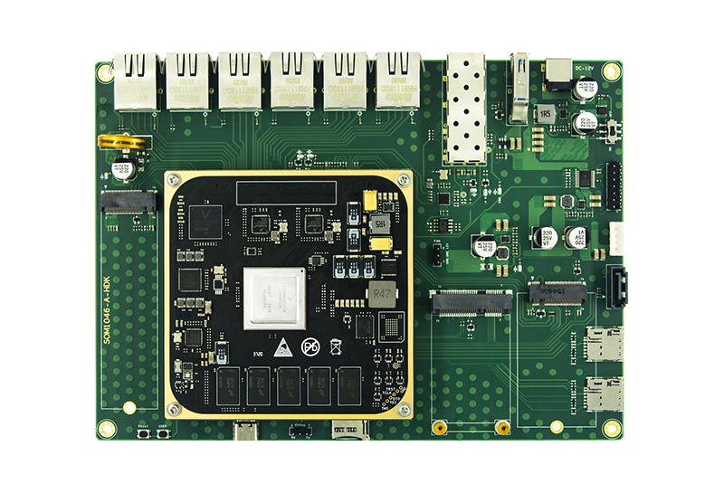
| Rigid board capacity |
| Number of layers: | 1-42 layers |
| Material: | FR4\high TG FR4\Lead free material\CEM1\CEM3\Aluminum\Metal core\PTFE\Rogers |
| Out layer Cu thickness: | 1-6OZ |
| Inner layer Cu thickness: | 1-4OZ |
| Maximum processing area: | 610*1100mm |
| Minimum board thickness: | 2 layers 0.3mm (12mil) 4 layers 0.4mm (16mil) 6 layers 0.8mm (32mil) 8 layers 1.0mm (40mil) 10 layers 1.1mm (44mil) 12 layers 1.3mm (52mil) 14 layers 1.5mm (59mil) 16 layers 1.6mm (63mil) |
| Minimum Width: | 0.076mm (3mil) |
| Minimum Space: | 0.076mm (3mil) |
| Minimum hole size (final hole): | 0.2mm |
| Aspect ratio: | 10:1 |
| Drilling hole size: | 0.2-0.65mm |
| Drilling tolerance: | +\-0.05mm(2mil) |
| PTH tolerance: | Φ0.2-1.6mm +\-0.075mm (3mil) Φ1.6-6.3mm+\-0.1mm(4mil) |
| NPTH tolerance: | Φ0.2-1.6mm +\-0.05mm(2mil) Φ1.6-6.3mm+\-0.05mm(2mil) |
| Finish board tolerance: | Thickness<0.8mm, Tolerance:+/-0.08mm |
| 0.8mm≤Thickness≤6.5mm,Tolerance+/-10% |
| Minimum soldermask bridge: | 0.076mm (3mil) |
| Twisting and bending: | ≤0.75% Min0.5% |
| Raneg of TG: | 130-215℃ |
| Impedance tolerance: | +/-10%,Min+/-5% |
| Surface Treatment: | HASL, LF HASL |
| Immersion Gold, Flash Gold,Gold finger |
| Immersion Silver, Immersion Tin,OSP |
| Selective Gold Plating, Gold thickness up to 3um(120u”) |
| Carbon Print, Peelable S/M,ENEPIG |
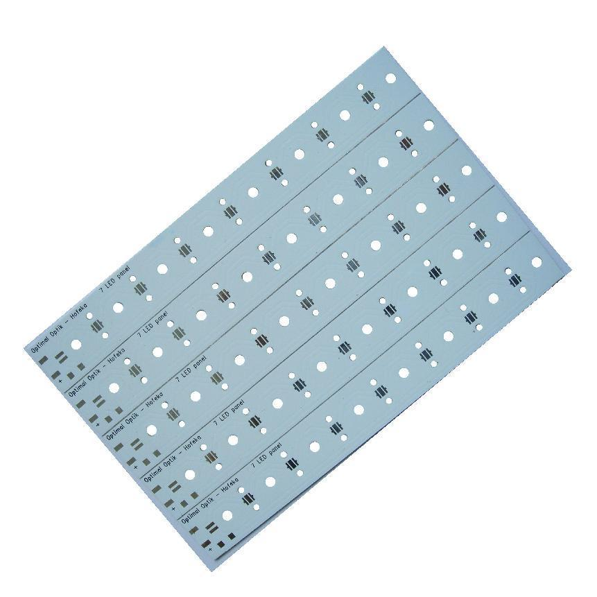
| Aluminum board capacity |
| Number of layers: | Single layer, double layers |
| Maximum board size: | 1500*600mm |
| Board thickness: | 0.5-3.0mm |
| Copper thickness: | 0.5-4oz |
| Minimum hole size: | 0.8mm |
| Minimum width: | 0.1mm |
| Minimum space: | 0.12mm |
| Minimum pad size: | 10 micron |
| Surface finish: | HASL,OSP,ENIG |
| Shaping: | CNC, Punching, V-cut |
| Equipement: | Universal Tester |
| Flying Probe Open/Short Tester |
| High power Microscope |
| Solderability Testing Kit |
| Peel Strength tester |
| High Volt Open & Short tester |
| Cross Section Molding Kit With Polisher |
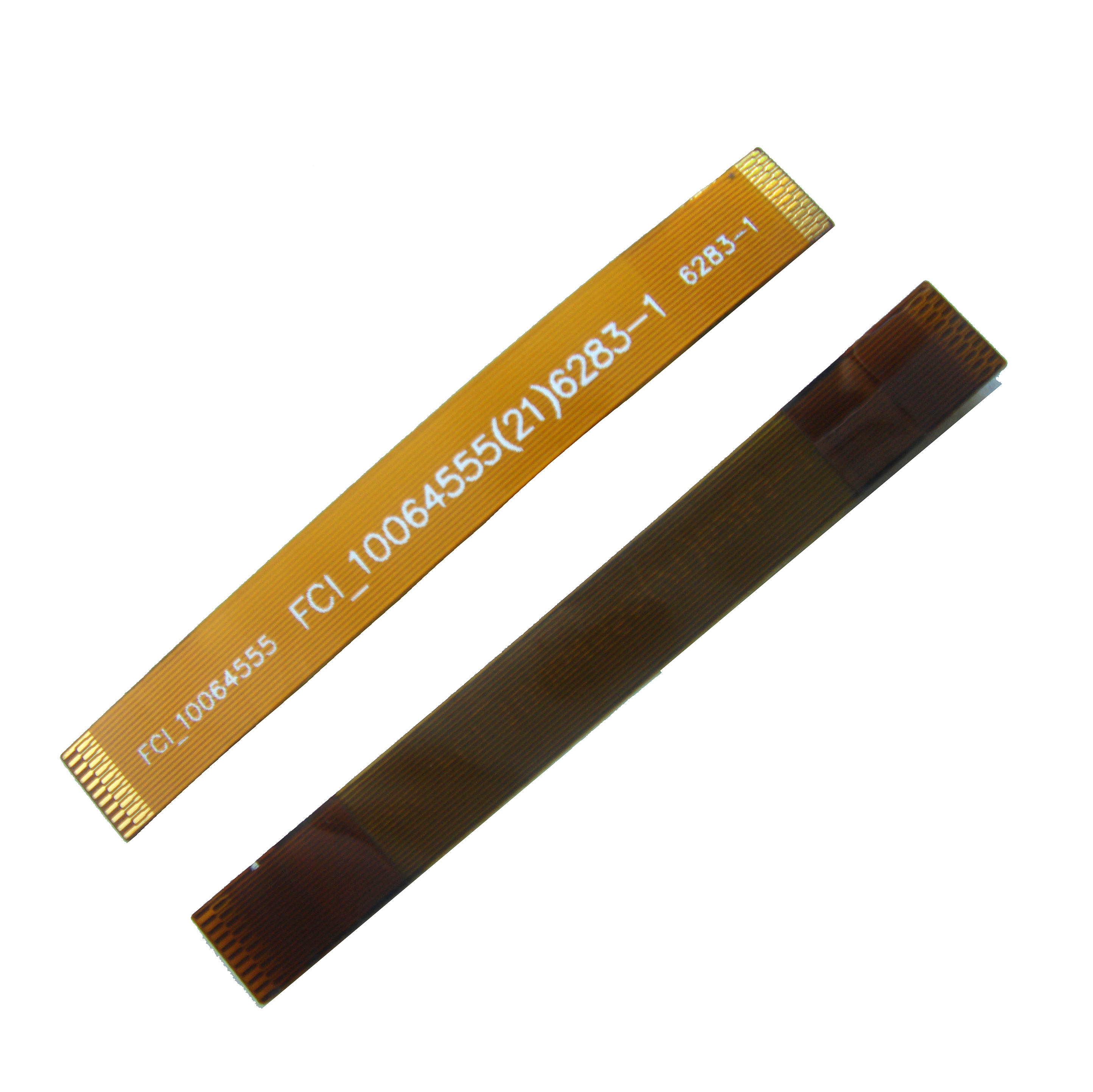
| FPC Capacity |
| Layers: | 1-8 layers |
| Board thickness: | 0.05-0.5mm |
| Copper thickness: | 0.5-3OZ |
| Minimum Width: | 0.075mm |
| Minimum space: | 0.075mm |
| In through hole size: | 0.2mm |
| Minimum laser hole size: | 0.075mm |
| Minimum punching hole size: | 0.5mm |
| Soldermask tolerance: | +\-0.5mm |
| Minimum routing dimension tolerance: | +\-0.5mm |
| Surface finish: | HASL,LF HASL, Immersion Silver, Immersion Gold,Flash Gold, OSP |
| Shaping: | Punching, Laser, Cut |
| Equipement: | Universal Tester |
| Flying Probe Open/Short Tester |
| High power Microscope |
| Solderability Testing Kit |
| Peel Strength tester |
| High Volt Open & Short tester |
| Cross Section Molding Kit With Polisher |
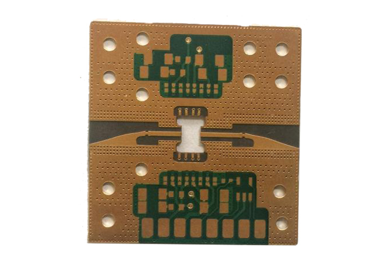
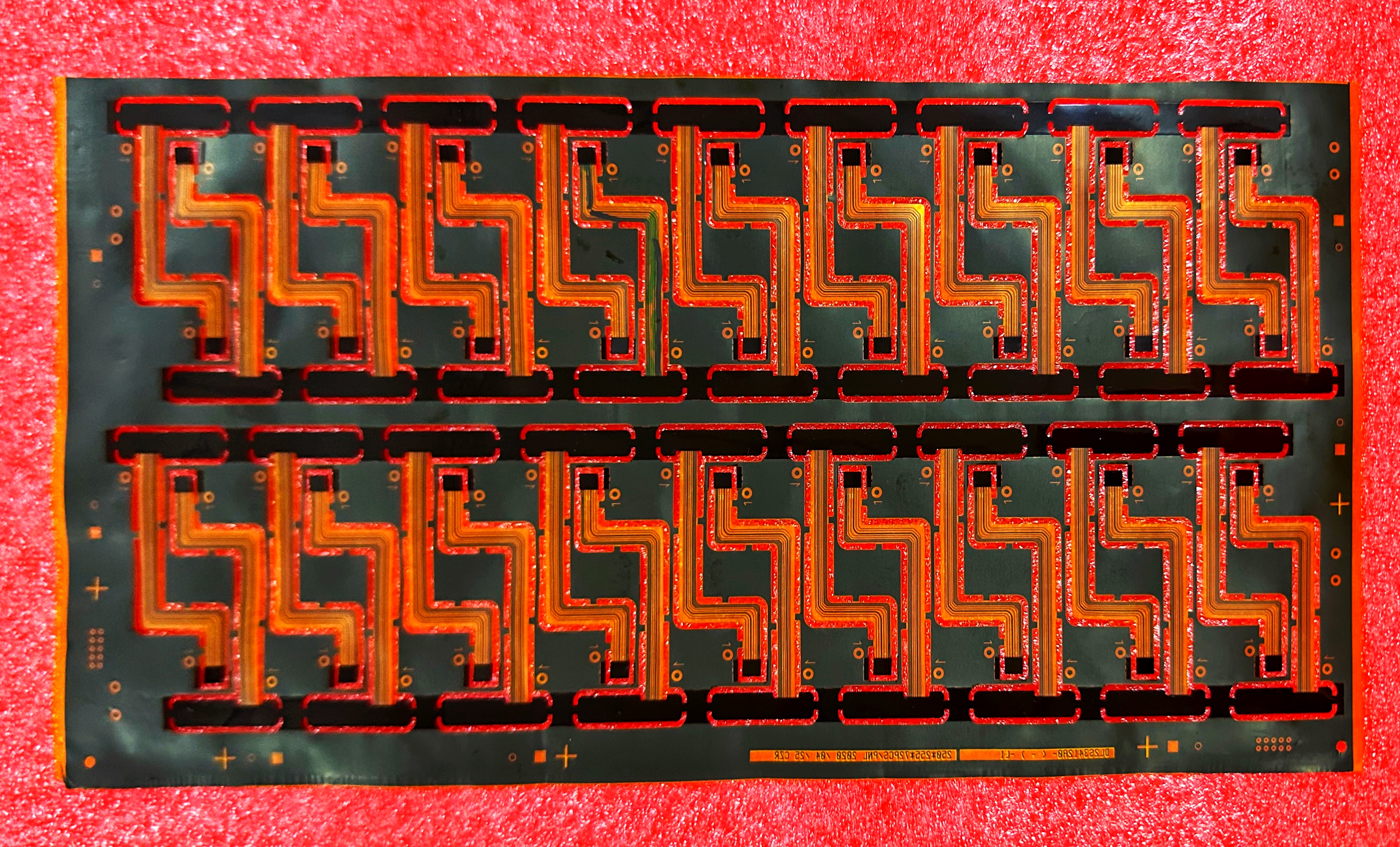
| Rigid&flex capacity |
| Layers: | 1-28 layers |
| Material type: | FR-4(High Tg, Halogen Free, High Frequency) PTFE, BT, Getek, Aluminium base,Copper base,KB, Nanya, Shengyi, ITEQ, ILM, Isola, Nelco, Rogers, Arlon |
| Board thickness: | 6-240mil/0.15-6.0mm |
| Copper thickness: | 210um (6oz) for inner layer 210um (6oz) for outer layer |
| Min mechanical drill size: | 0.2mm/0.08” |
| Aspect ratio: | 2:1 |
| Max panel size: | Sigle side or double sides:500mm*1200mm |
| Multilayer layers:508mm X 610mm (20″ X 24″) |
| Min line width/space: | 0.076mm / 0.076mm (0.003″ / 0.003″)/ 3mil/3mil |
| Via hole type: | Blind / Buried / Plugged(VOP,VIP…) |
| HDI / Microvia: | YES |
| Surface finish: | HASL, LF HASL |
| Immersion Gold, Flash Gold,Gold finger |
| Immersion Silver, Immersion Tin,OSP |
| Selective Gold Plating, Gold thickness up to 3um(120u”) |
| Carbon Print, Peelable S/M,ENEPIG |
| Shaping: | CNC, Punching, V-cut |
| Equipement: | Universal Tester |
| Flying Probe Open/Short Tester |
| High power Microscope |
| Solderability Testing Kit |
| Peel Strength tester |
| High Volt Open & Short tester |
| Cross Section Molding Kit With Polisher |