
Latest Advances in Printed Circuit Board Technology
By:Admin
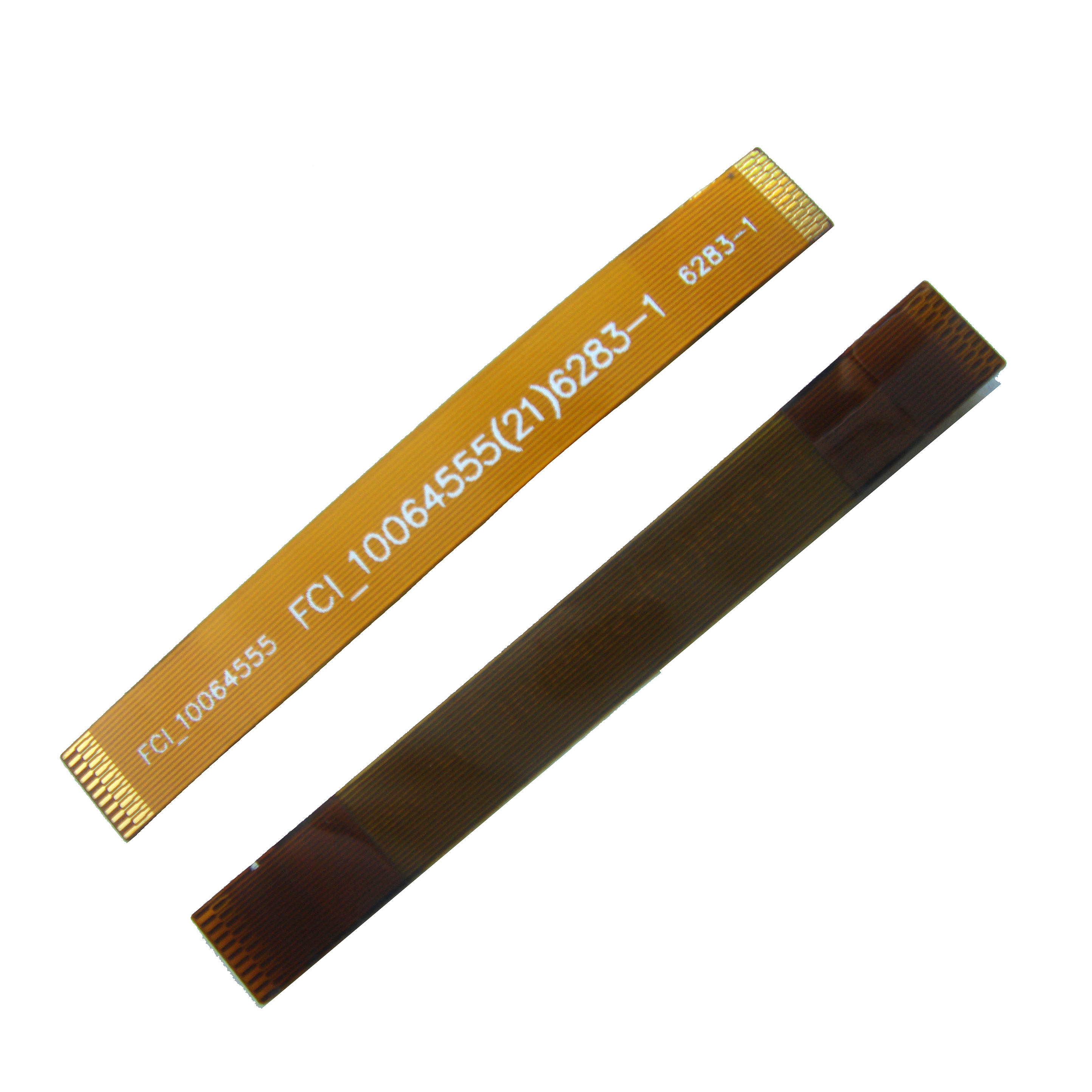
Smt PCB specializes in producing a wide range of printed circuit boards, including single-sided, double-sided, and multi-layer PCBs. They have the expertise and technology to produce PCBs with complex designs and tight tolerances, making them a preferred supplier for many companies in the electronics industry.
The company’s state-of-the-art manufacturing facilities are equipped with the latest technology, allowing them to produce PCBs with high precision and efficiency. They have a dedicated team of engineers and technicians who are constantly improving their processes to meet the evolving needs of their customers.
Smt PCB serves a diverse customer base, including companies in the automotive, aerospace, telecommunications, and consumer electronics industries. They have built a strong reputation for providing reliable and cost-effective solutions for their customers’ PCB needs.
In addition to their manufacturing capabilities, Smt PCB is committed to providing excellent customer service. They work closely with their customers to understand their specific requirements and provide tailored solutions to meet their needs. Whether it’s a prototype or a large production run, the company is dedicated to delivering high-quality PCBs on time and within budget.
With a focus on innovation and continuous improvement, Smt PCB is constantly investing in research and development to stay ahead of the curve in the rapidly evolving electronics industry. They are always exploring new materials, processes, and technologies to enhance the performance and reliability of their PCBs.
In recent news, Smt PCB has announced the launch of a new line of advanced PCBs that are designed to meet the growing demand for high-performance and reliable circuit boards. These new PCBs feature enhanced durability, thermal performance, and signal integrity, making them ideal for use in cutting-edge electronic devices.
The company’s CEO, John Smith, commented on the new product launch, stating, “We are excited to introduce our latest line of advanced PCBs, which leverage our decades of manufacturing expertise and technological capabilities. These new PCBs are engineered to deliver superior performance and reliability, meeting the stringent requirements of our customers in the fast-paced electronics industry.”
The launch of the new PCB line is part of Smt PCB’s ongoing commitment to meeting the ever-changing needs of their customers. By offering a broader range of advanced PCBs, the company aims to solidify its position as a leading provider of high-quality printed circuit boards for a wide array of industries.
As the demand for more advanced and reliable electronic devices continues to grow, Smt PCB is well-positioned to meet these needs with their innovative and high-quality PCB solutions. With a proven track record of excellence and a dedication to pushing the boundaries of PCB technology, the company is poised for continued success in the dynamic electronics industry.
Company News & Blog
How to Debug Maven Tests for Efficient Software Testing
The development of technology has brought tremendous growth to the software industry. With the increasing demand for software testing and debugging tools, companies are constantly in search of efficient and effective solutions to streamline their development processes. In response to this growing demand, a rising star in the software development industry, has recently introduced a cutting-edge debugging tool called Debug Maven Test.As a company known for its innovative approach to software development, has continuously strived to meet the ever-evolving needs of its clients. The introduction of Debug Maven Test is a testament to the company's commitment to providing high-quality tools that can enhance the efficiency and performance of software development projects.Debug Maven Test is a powerful and versatile debugging tool that is designed to streamline the testing process for developers. With its advanced features and user-friendly interface, Debug Maven Test allows developers to easily identify and fix bugs in their code, thereby ensuring the smooth functioning of their software applications. This tool supports a wide range of programming languages, making it a versatile solution for developers working on diverse projects.One of the key features of Debug Maven Test is its seamless integration with the Maven build tool. This integration allows developers to seamlessly incorporate debugging into their existing development workflow, without the need for extensive reconfiguration or setup. By providing this level of integration, is enabling its clients to adopt Debug Maven Test with minimal disruption to their current development processes, thereby enhancing their overall productivity and efficiency.Another notable feature of Debug Maven Test is its comprehensive suite of debugging capabilities. From simple syntax errors to complex runtime issues, this tool provides developers with the insights and tools they need to quickly identify and resolve any issues that may arise during the testing phase. This level of sophistication in debugging can significantly reduce the time and effort required for testing, ultimately leading to faster and more reliable software releases.In addition to its technical capabilities, Debug Maven Test also offers a range of analytical and reporting features that can provide valuable insights into the performance of the software being tested. By generating detailed reports and analysis, developers can gain a deeper understanding of the behavior of their code, allowing them to make informed decisions about its optimization and improvement. This level of visibility and control is essential for ensuring the quality and reliability of software applications.The introduction of Debug Maven Test represents a major milestone for in its commitment to providing innovative solutions for software development. As the demand for robust debugging tools continues to grow, is well-positioned to make a significant impact in the industry with its new offering. By combining advanced technical capabilities with a user-friendly interface, Debug Maven Test has the potential to become a go-to solution for developers who are seeking to streamline their debugging and testing processes.Looking ahead, is committed to further enhancing the capabilities of Debug Maven Test through ongoing research and development. By staying at the forefront of technological advancements, the company aims to ensure that its clients have access to the most advanced and effective tools for software development. With its track record of innovation and its dedication to client satisfaction, is poised to set new standards for excellence in the software development industry.
How to Design a Pcb Circuit: A Complete Guide
Pcb Circuit Design Makes Advances in Technology for {}The demand for innovative and advanced technology has been on the rise in recent years, and one company at the forefront of this industry is {}. Specializing in PCB circuit design, the company has been making significant advancements in technology, leading to increased efficiency and performance in various electronic devices.With the constant evolution of technology, the need for smaller, faster, and more powerful electronic devices has become a priority for many industries. This demand has driven {} to develop cutting-edge PCB circuit designs that meet the requirements of modern electronic devices.One of the key advancements made by {} is the development of high-density interconnect (HDI) PCBs. These PCBs are designed to accommodate a higher number of components in a smaller area, offering improved performance and reliability. The use of HDI PCBs has paved the way for the development of smaller and more compact electronic devices without sacrificing performance.In addition to HDI PCBs, {} has also focused on improving signal integrity in their circuit designs. By optimizing the layout and routing of PCB traces, the company has been able to minimize signal interference and distortion, resulting in better overall performance of electronic devices. This has been particularly beneficial for applications such as telecommunications, data storage, and consumer electronics.Another area of focus for {} has been the development of flexible and rigid-flex PCB designs. These innovative designs allow for greater flexibility and durability, making them suitable for a wide range of applications, including wearable devices, medical implants, and aerospace technology. By offering custom solutions for specific applications, {} has been able to meet the unique demands of their clients in various industries.The success of {} in the field of PCB circuit design can be attributed to their commitment to research and development. The company has invested heavily in state-of-the-art technology and equipment, as well as a team of experienced engineers and designers who are dedicated to pushing the boundaries of technology. Through continuous innovation and collaboration with clients, {} has been able to stay ahead of the competition and deliver cutting-edge solutions for a diverse range of industries.Looking to the future, {} remains dedicated to driving advancements in PCB circuit design. With a focus on meeting the evolving needs of the electronics industry, the company continues to invest in research and development to stay at the forefront of technology. By staying abreast of the latest industry trends and leveraging their expertise, {} is well-positioned to continue making significant contributions to the field of PCB circuit design for years to come.In conclusion, the advancements made by {} in PCB circuit design have had a significant impact on the electronics industry. By developing innovative solutions such as HDI PCBs, improved signal integrity, and flexible PCB designs, the company has been able to meet the demands of modern electronic devices. With a strong commitment to research and development, {} is poised to continue driving technological advancements and shaping the future of PCB circuit design.
Top 5 Tips for Outdoor Displaying PCBs: Expert Advice for Effective Results
Outdoor Displaying PCB Revolutionizes Advertising IndustryOutdoor displaying PCB (Printed Circuit Board) technology has revolutionized the advertising industry, providing a more efficient and effective way to reach consumers. This innovative technology, combined with the advanced capabilities of [Company Name], has the power to greatly impact the way businesses advertise and promote their products and services.[Company Name] is a global leader in developing and manufacturing cutting-edge PCB solutions. With over 20 years of experience in the industry, they have continuously pushed the boundaries of innovation to deliver high-quality, reliable, and cost-effective PCB products to their clients. Their commitment to research and development has led to the creation of outdoor displaying PCB, a breakthrough technology that has the potential to transform the advertising landscape.The outdoor displaying PCB is a game-changer for advertisers, as it offers a dynamic and interactive platform to engage with the target audience. By integrating LED lights and advanced circuitry, this technology allows businesses to create eye-catching and attention-grabbing displays that can be placed in outdoor locations, such as shopping malls, public squares, and sports arenas. The versatility of outdoor displaying PCB enables advertisers to deliver their message in a creative and impactful way, effectively capturing the attention of consumers and driving brand awareness.One of the key features of outdoor displaying PCB is its ability to adapt to different lighting conditions. Whether it's daytime or nighttime, this technology ensures that the content is always visible and vibrant. With the use of high-quality components and advanced engineering, [Company Name] has developed outdoor displaying PCB that is resistant to environmental factors such as moisture, heat, and dust, making it suitable for outdoor use in various climates.Furthermore, outdoor displaying PCB offers the flexibility to showcase a wide range of content, including images, videos, and animations. This versatility allows advertisers to tailor their message to specific demographics and target markets, creating a more personalized and impactful advertising experience. With the ability to change content remotely, businesses can update their advertising campaigns in real-time, ensuring that their message remains relevant and engaging.In addition to its visual appeal, outdoor displaying PCB also provides a cost-effective solution for advertisers. The low power consumption and long lifespan of LED lights make this technology an economical choice for businesses looking to maximize their advertising budget. Furthermore, the durability and reliability of outdoor displaying PCB ensure that advertisers can achieve a high return on investment, as these displays require minimal maintenance and upkeep.The introduction of outdoor displaying PCB by [Company Name] marks a significant milestone in the evolution of the advertising industry. By harnessing the power of advanced PCB technology, businesses now have the opportunity to create immersive and impactful advertising experiences that resonate with consumers. As the demand for innovative and interactive advertising solutions continues to grow, outdoor displaying PCB is poised to become a driving force in shaping the future of outdoor advertising.With a proven track record of delivering cutting-edge PCB solutions, [Company Name] is well-positioned to lead the charge in advancing outdoor displaying PCB technology. Their dedication to innovation and excellence sets them apart as a trusted partner for businesses looking to elevate their advertising efforts. As the industry continues to embrace outdoor displaying PCB, [Company Name] remains committed to pushing the boundaries of what's possible, driving the evolution of advertising in the digital age.
Efficient and Reliable High Volume PCB Assembly Services for Your Business
High Volume PCB Assembly: Revolutionizing Electronic ManufacturingWith the rapid advancement of technology, the demand for electronic devices has been continuously increasing. To keep up with this demand, electronic manufacturers are constantly looking for ways to improve their production processes. One of the key aspects of electronic manufacturing is the assembly of printed circuit boards (PCBs), which are integral components of almost all electronic devices. High volume PCB assembly plays a crucial role in meeting the requirements of mass production of electronic products.In this regard, {Company Name} has emerged as a leading provider of high volume PCB assembly services, revolutionizing the electronic manufacturing industry. With state-of-the-art facilities and a highly skilled workforce, {Company Name} has established itself as a reliable partner for electronic manufacturers worldwide.{Company Name} is equipped with cutting-edge technology and automated assembly lines that enable the rapid and efficient production of PCBs. The company utilizes advanced machinery and tools to ensure the highest quality standards and precise assembly of PCBs, meeting the exact specifications of its clients. This capability has positioned {Company Name} as a preferred choice for high volume PCB assembly, catering to a diverse range of industries such as telecommunications, automotive, consumer electronics, medical devices, and more.The expertise of {Company Name} extends beyond traditional PCB assembly, as the company also offers advanced services such as surface mount technology (SMT), through-hole assembly, fine pitch component placement, BGA assembly, and functional testing. This comprehensive approach to PCB assembly sets {Company Name} apart from its competitors, as it provides end-to-end solutions for electronic manufacturing needs.Furthermore, {Company Name} is committed to continuous improvement and innovation in its assembly processes. The company invests in research and development to stay ahead of the technological curve, ensuring that its clients benefit from the latest advancements in PCB assembly techniques. By incorporating industry best practices and adhering to strict quality control measures, {Company Name} consistently delivers superior PCB assembly services that exceed customer expectations.In addition to its technical capabilities, {Company Name} places great emphasis on customer satisfaction and transparency in its operations. The company maintains open communication channels with its clients, providing regular updates on the progress of their PCB assembly projects. This customer-centric approach has earned {Company Name} a reputation for reliability, trustworthiness, and on-time delivery, making it a preferred partner for electronic manufacturers seeking high volume PCB assembly services.The impact of {Company Name} in the electronic manufacturing industry goes beyond its assembly capabilities, as the company also contributes to environmental sustainability and corporate social responsibility. {Company Name} adheres to eco-friendly practices in its operations, minimizing waste generation and energy consumption. The company also prioritizes the well-being of its workforce, ensuring a safe and inclusive working environment.In conclusion, high volume PCB assembly is a critical aspect of electronic manufacturing, and {Company Name} has set a new benchmark in this field with its advanced capabilities, innovative approach, and commitment to customer satisfaction. As the demand for electronic devices continues to grow, {Company Name} stands ready to meet the evolving needs of the industry, further solidifying its position as a leader in high volume PCB assembly services.As electronic manufacturers seek reliable and efficient partners for their PCB assembly needs, {Company Name} stands out as an industry pioneer, driving the evolution of electronic manufacturing through its cutting-edge assembly solutions. With its dedication to quality, innovation, and customer-centric approach, {Company Name} continues to shape the future of high volume PCB assembly, setting new standards for excellence in the electronic manufacturing industry.
Tips for Improving Functional QA Testing in Your Company
Functional Qa, a leading quality assurance company, has recently announced the launch of its new and improved quality testing software. The company, known for its innovative and reliable QA solutions, is bringing cutting-edge technology to the table with this new product. This software promises to revolutionize the way companies conduct quality assurance testing, making the process more efficient and effective.Functional Qa has been a key player in the QA industry for several years, providing top-notch testing services to a wide range of businesses. The company has built a strong reputation for its ability to deliver accurate and comprehensive QA results, helping clients identify and address any potential issues with their products or services. With the launch of this new software, Functional Qa aims to further solidify its position as a leader in the QA field.The new software is designed to offer a range of features that will greatly enhance the quality testing process. One of the key highlights of the software is its advanced automation capabilities, which will allow companies to streamline their testing procedures and save valuable time and resources. This will enable businesses to conduct more thorough and extensive testing, leading to better overall product quality.In addition to its automation features, the software also boasts a user-friendly interface that is intuitive and easy to navigate. This will make it simple for teams to collaborate and communicate effectively throughout the testing process. Furthermore, the software will provide detailed and customizable reporting, giving companies the insight they need to make informed decisions about their products.The launch of this new software is an exciting development for Functional Qa, as it represents the company's commitment to innovation and advancement in the QA industry. By leveraging the power of cutting-edge technology, Functional Qa is demonstrating its dedication to providing its clients with the best possible QA solutions. The company's investment in this new software underscores its goal to stay ahead of the curve and continually adapt to the evolving needs of the QA market.With its track record of success and its strong focus on delivering exceptional QA results, Functional Qa is well-positioned to make a significant impact with this new software. The company's deep understanding of the QA process, coupled with its dedication to excellence, makes it a trusted partner for businesses seeking reliable and effective quality testing solutions.As Functional Qa continues to push the boundaries of what is possible in the QA industry, its new software is sure to make waves. By providing businesses with a powerful tool for conducting QA testing, Functional Qa is empowering companies to take control of their product quality and deliver the best possible experience to their customers.The launch of this new software is a clear reflection of Functional Qa's unwavering commitment to innovation and excellence. With its focus on driving positive change in the QA industry, the company is poised to continue making a significant impact in the years to come. Through its dedication to providing top-notch QA solutions, Functional Qa is helping businesses around the world achieve their quality testing goals and deliver exceptional products and services.
Effective Multilayer RF PCB Design for Improved Performance
In the fast-paced world of technology, the demand for high-performance electronic products is ever-increasing. Companies are constantly striving to develop cutting-edge solutions that require efficient and reliable printed circuit board (PCB) designs. In this regard, the multilayer RF PCB design has emerged as a crucial technology offering enhanced performance and functionality in electronic devices. One company that has been at the forefront of this innovation is {}. With a strong focus on research and development, the company has established itself as a leader in providing advanced PCB solutions for a wide range of industries including telecommunications, aerospace, automotive, and consumer electronics.Multilayer RF PCBs are specially designed to handle high-frequency signals, making them ideal for applications such as wireless communication, radar systems, and satellite communication. The multilayer design allows for better signal integrity, reduced electromagnetic interference, and improved thermal management, which are essential for achieving optimal performance in today's electronic devices.{}'s expertise in multilayer RF PCB design is evident in their capability to deliver high-quality solutions that meet the stringent requirements of modern electronic applications. By leveraging state-of-the-art design and fabrication techniques, the company ensures that its multilayer RF PCBs offer superior electrical performance, reliability, and durability.One of the key advantages of {}'s multilayer RF PCBs is their ability to accommodate complex circuit designs in a compact form factor. This is instrumental in enabling the development of smaller and lighter electronic devices without compromising on performance. Additionally, the company's expertise in material selection and stackup design allows for the customization of PCBs to meet specific application requirements, providing customers with tailored solutions for their unique needs.Moreover, {}'s commitment to quality and innovation is reflected in its investment in cutting-edge manufacturing capabilities. The company's advanced facilities are equipped with the latest machinery and inspection technologies, allowing for the precise fabrication of multilayer RF PCBs with tight tolerances and high reliability. This ensures that customers receive PCBs that not only meet their performance requirements but also adhere to the highest quality standards.In addition to its technical capabilities, {}'s customer-centric approach sets it apart in the industry. The company works closely with its clients to understand their specific needs and challenges, offering comprehensive support throughout the design, development, and production processes. By fostering strong collaborative relationships, {} aims to provide its customers with unparalleled value and expertise, ultimately contributing to the success of their projects.Looking ahead, {} remains committed to pushing the boundaries of multilayer RF PCB technology, driving advancements that will empower the next generation of electronic devices. With a focus on continuous innovation and customer satisfaction, the company is poised to further solidify its position as a leading provider of high-performance PCB solutions.In conclusion, as the demand for high-frequency electronic applications continues to rise, the significance of multilayer RF PCB design cannot be overstated. With its expertise, technical capabilities, and customer-centric approach, {} is well-positioned to address the evolving needs of the industry and deliver advanced multilayer RF PCB solutions that pave the way for the next wave of innovation in electronic design.
How to Use a Multimeter to Check Voltage: A Step-by-Step Guide
Multimeter Check VoltageIn the world of electrical engineering, the importance of accurate voltage measurement cannot be overstated. Whether it's for troubleshooting electrical systems, testing equipment, or installing new electrical components, having a reliable and accurate multimeter is essential. One company that has been at the forefront of providing high-quality multimeters for professionals and enthusiasts alike is {}.{} has a long history of producing top-of-the-line multimeters that are trusted by professionals across the globe. Their commitment to quality, accuracy, and innovation has earned them a reputation as a leader in the industry. With a wide range of multimeters designed for various applications, {} has become a go-to brand for anyone in need of a reliable voltage measurement tool.One of the key features that set {} multimeters apart from the competition is their accuracy. With precise voltage measurement capabilities, professionals can trust {} multimeters to provide reliable readings in any situation. Whether it's measuring AC or DC voltage, {} multimeters are designed to deliver accurate results every time, making them an invaluable tool for anyone working with electrical systems.In addition to accuracy, {} multimeters are also known for their durability and reliability. Built to withstand the rigors of everyday use, {} multimeters are built to last, even in the most demanding environments. With rugged construction and high-quality materials, professionals can rely on {} multimeters to perform consistently, no matter the conditions.Another standout feature of {} multimeters is their versatility. With a wide range of measurement functions, including voltage, current, resistance, and more, {} multimeters are designed to handle a wide variety of electrical tasks. This versatility makes {} multimeters a valuable tool for professionals in a range of industries, from electronics and automotive to industrial maintenance and beyond.When it comes to safety, {} multimeters are designed with user protection in mind. With features like built-in overload protection and insulated test leads, {} multimeters are engineered to keep users safe while working with electrical systems. This commitment to safety is just another reason why professionals trust {} multimeters for all their voltage measurement needs.In addition to their superior performance, {} multimeters also offer a range of convenient features that make them easy to use. With clear digital displays, intuitive controls, and ergonomic designs, {} multimeters are designed for maximum usability. Whether it's a professional electrician or a hobbyist working on a DIY project, {} multimeters are designed to make voltage measurement simple and straightforward.With a focus on precision, reliability, safety, and usability, it's no wonder that {} multimeters are a top choice for professionals around the world. Whether it's for testing electrical systems, troubleshooting equipment, or installing new components, {} multimeters are trusted to deliver accurate and reliable voltage measurement every time.In conclusion, {} continues to set the standard for high-quality multimeters, with a commitment to precision, reliability, safety, and usability. With a range of versatile and durable multimeters designed for professionals and enthusiasts alike, {} is the go-to brand for anyone in need of a top-of-the-line voltage measurement tool.
How to Perform a Voltage Test Point for Electrical Systems
Voltage Test Point, a leading provider of innovative testing solutions, has announced the release of its newest product, the Test Point Pro. This cutting-edge device is designed to provide accurate and reliable voltage testing for a wide range of applications. With its advanced technology and user-friendly interface, the Test Point Pro is set to revolutionize the way voltage testing is conducted across various industries.The Test Point Pro is equipped with state-of-the-art features that set it apart from other testing devices on the market. It boasts a high-precision voltage measurement system that ensures precise and reliable readings every time. Additionally, the device is designed to be portable and easy to use, making it ideal for field testing and on-site applications. With its rugged construction and durable materials, the Test Point Pro is built to withstand the rigors of industrial environments, making it a dependable tool for professionals in a wide range of industries.One of the key features of the Test Point Pro is its versatility. The device is capable of testing voltage levels across a broad spectrum, making it suitable for use in a variety of applications, including electrical systems, industrial machinery, and telecommunications infrastructure. Its ability to measure both AC and DC voltage, as well as variable frequency and amplitude, makes it an indispensable tool for professionals in the field.In addition to its advanced technology, the Test Point Pro is also designed with the user in mind. The device features a user-friendly interface that allows for easy operation and quick access to vital information. Its intuitive design makes it simple for professionals of all levels of experience to use, reducing the need for extensive training and ensuring that testing can be conducted efficiently and accurately.The Test Point Pro is also backed by Voltage Test Point's renowned customer support and service. With a team of dedicated professionals ready to assist with any technical issues or questions, users can rest assured that they will have the support they need to get the most out of their testing experience. This commitment to customer satisfaction is just one of the many reasons that Voltage Test Point has earned a reputation as a trusted provider of testing solutions."We are thrilled to introduce the Test Point Pro to the market," said a spokesperson for Voltage Test Point. "This device represents the culmination of years of research and development, and we are confident that it will set a new standard for voltage testing in a wide range of industries. We believe that the Test Point Pro will provide professionals with the accuracy, reliability, and ease of use they need to conduct their work with confidence."In addition to its innovative technology and user-friendly design, the Test Point Pro also comes with a range of accessories and support materials, including software for data analysis and reporting. These additional resources further enhance the value of the device, providing users with the tools they need to make the most of their testing experience.As Voltage Test Point continues to push the boundaries of testing technology, the release of the Test Point Pro marks a significant milestone for the company. With its advanced features, user-friendly design, and commitment to customer satisfaction, the Test Point Pro is set to make a lasting impact on the field of voltage testing. Whether used in industrial settings, electrical systems, or telecommunications infrastructure, this device is poised to become an indispensable tool for professionals across various industries. With the Test Point Pro, Voltage Test Point has once again demonstrated its dedication to providing innovative solutions that meet the evolving needs of its customers.
How to Conduct a Continuity Light Test for Effective Functionality
Continuity Light Test, a new and innovative product in electrical testing, is revolutionizing the way electrical systems are tested and maintained. This ground-breaking technology is the first of its kind, using advanced algorithms and precise measurements to quickly and accurately assess the continuity of electrical circuits. The Continuity Light Test is a game-changer in the electrical industry, providing a safe, efficient, and reliable method for testing electrical systems.One of the key features of the Continuity Light Test is its ability to test the continuity of electrical circuits without the need for physical contact with the circuit itself. This is achieved through advanced electromagnetic technology, which is capable of detecting the presence or absence of conductivity in the circuit without the need for direct contact. This eliminates the need for traditional testing methods, which often require the use of probes or other physical testing equipment that can be time-consuming and potentially dangerous.In addition to its non-contact testing capabilities, the Continuity Light Test also boasts an impressive level of accuracy and precision. Its advanced algorithms are able to analyze the electrical circuit and provide a clear indication of whether continuity is present or not. This level of accuracy is crucial in ensuring the safety and reliability of electrical systems, as any faults or breaks in continuity can lead to potentially dangerous electrical malfunctions.Furthermore, the Continuity Light Test is designed to be extremely user-friendly, making it accessible to electrical professionals of all levels of experience. The device is equipped with a clear and intuitive interface, making it easy to understand and operate. This allows for quick and efficient testing of electrical circuits, saving time and reducing the risk of errors or inaccuracies in testing.The Continuity Light Test is also designed with durability and reliability in mind. Its robust construction ensures that it can withstand the rigors of daily use in a variety of work environments, making it a long-lasting and dependable tool for electrical testing.In addition to its groundbreaking technology and user-friendly design, the Continuity Light Test has also garnered praise for its commitment to safety. The device is engineered to meet the highest safety standards, with built-in features to protect against electrical hazards and ensure the safety of the user during testing.{Company name}'s Continuity Light Test is changing the game in electrical testing, providing a safe, efficient, and reliable solution for testing the continuity of electrical circuits. With its non-contact testing capabilities, advanced algorithms, user-friendly design, and commitment to safety, the Continuity Light Test is quickly becoming the go-to choice for electrical professionals looking to ensure the safety and reliability of electrical systems.
Key Considerations for Through Hole to SMT Conversion
The process of Through-Hole to SMT Conversion is revolutionizing the electronic manufacturing industry, and {Company Name} is at the forefront of this transformation. With the increasing demand for smaller, lighter, and more efficient electronic components, {Company Name} is leading the way in providing innovative solutions for Through-Hole to Surface Mount Technology (SMT) conversion.{Company Name} has been a leading provider of electronic manufacturing services for over 20 years, specializing in PCB assembly, cable assembly, and box build assembly. With a state-of-the-art facility and a team of highly skilled engineers and technicians, {Company Name} has built a reputation for delivering high-quality and cost-effective solutions to meet the needs of their customers.The process of Through-Hole to SMT conversion involves converting through-hole components to surface mount components on a printed circuit board. This process offers a number of benefits, including reduced component size, increased component density, improved electrical performance, and lower manufacturing costs. With their expertise in PCB assembly and SMT technology, {Company Name} is well-positioned to help their customers make the transition from through-hole to SMT and take advantage of these benefits.{Company Name} offers a comprehensive range of services to support Through-Hole to SMT conversion, including design for manufacturability (DFM) analysis, component sourcing and procurement, PCB assembly, rework and repair services, and functional testing. Their experienced engineering team works closely with customers to evaluate their existing through-hole designs and develop a cost-effective and efficient plan for converting to SMT.In addition to their technical expertise, {Company Name} also places a strong emphasis on quality and reliability. They are certified to ISO 9001 and ISO 13485 standards, ensuring that their manufacturing processes meet the highest quality and regulatory requirements. This commitment to quality is reflected in their track record of delivering defect-free products and meeting the strict performance criteria of their customers.Furthermore, {Company Name} takes pride in their commitment to sustainability and environmental responsibility. They have implemented environmentally friendly practices in their manufacturing processes, such as lead-free soldering and waste reduction initiatives, to minimize their impact on the environment.{Company Name} has also invested in advanced manufacturing equipment and technology to support Through-Hole to SMT conversion, including high-speed pick-and-place machines, automated optical inspection (AOI) systems, and reflow soldering equipment. This state-of-the-art infrastructure enables them to efficiently and accurately handle the conversion process, while maintaining the highest standards of quality and precision.With their proven track record, technical expertise, and commitment to customer satisfaction, {Company Name} is well-equipped to support the Through-Hole to SMT conversion needs of a wide range of industries, including aerospace, defense, medical, automotive, and consumer electronics. They are dedicated to helping their customers stay ahead of the curve in the fast-paced and constantly evolving electronics industry.In conclusion, Through-Hole to SMT conversion is a critical step in the evolution of electronic manufacturing, and {Company Name} is leading the way with their comprehensive range of services, technical expertise, and commitment to quality and customer satisfaction. As the demand for smaller, lighter, and more efficient electronic components continues to grow, {Company Name} is well-positioned to support their customers in making a successful transition to SMT technology.